Review Of 4 Layers Pcb References. It consists of a thick core (about 42 mils) and 2 prepreg layers (7 mils each). The four layers in a 4 layer pcb are the top layer, the bottom layer, and two inner layers.
4 Layer PCB Layout Tutorial,Stackup design,and Cost of manufacturing from www.raypcb.com
@kris usually 4 layer pcbs use one internal plane for power, one for ground, but having two grounds will improve signal integrity and reduce emi if you can route them. The difference is not stark for all boards, but the four layer board will allow you to route signal, power, and ground, directly over each other in a larger variety of ways. Ground layers should be unbroken all high.
The Four Layer Board Adds Significantly More Routing Options In The Internal Layers As Compared To The Two Layer Board, And Often Some Portion Of The Internal Layers Is Used As Ground Plane Or Power Plane, To Achieve Better Signal Integrity, Higher Signaling Frequencies, Lower Emi, And.
The difference is not stark for all boards, but the four layer board will allow you to route signal, power, and ground, directly over each other in a larger variety of ways. Here are some specific design considerations to keep in. Choosing the best materials , setting layer dimensions, arranging the stackup, selecting the number, types, sizes and best locations for vias are all.
Factors Such As Low Emi And Noise Coupling Etc.
A four layer board will give better performance. There are 4 primary wiring layers, such as the top. The wiring is made of copper.
Bottom, Vcc, And Gnd Layers.
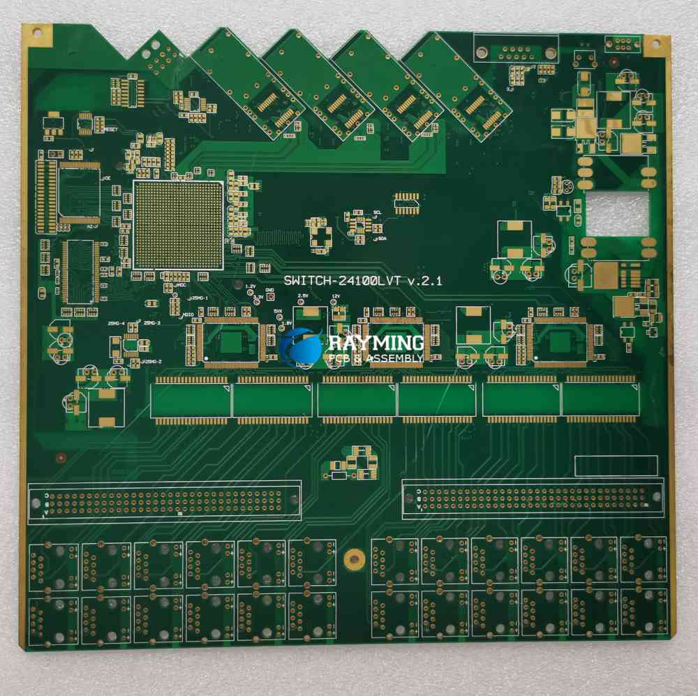
Web a 4 layer pcb layout is a printed circuit board design that consists of four layers of conductive material separated by insulating layers. These layers are connected through blind or buried holes. These 4 layers are sandwiched between two insulating layers, the substrate.
The 4 Layers Of Pcbs Are Then Laminated Together To Create A Single Board.
How to design a 4 layer pcb board. The layers are stacked on top of each other and separated by a thin layer of insulation. Top, as well as lower layers, are the external layers where we are positioning parts as well as directing.
Hi, I Shall Try And Answer Your Questions Within Your Original Text:
Add and delete inner layer; Web 4 layer pcb means there are 4 layers to rout electrical signals: There are two types are dielectric layers between copper layers.


No comments:
Post a Comment